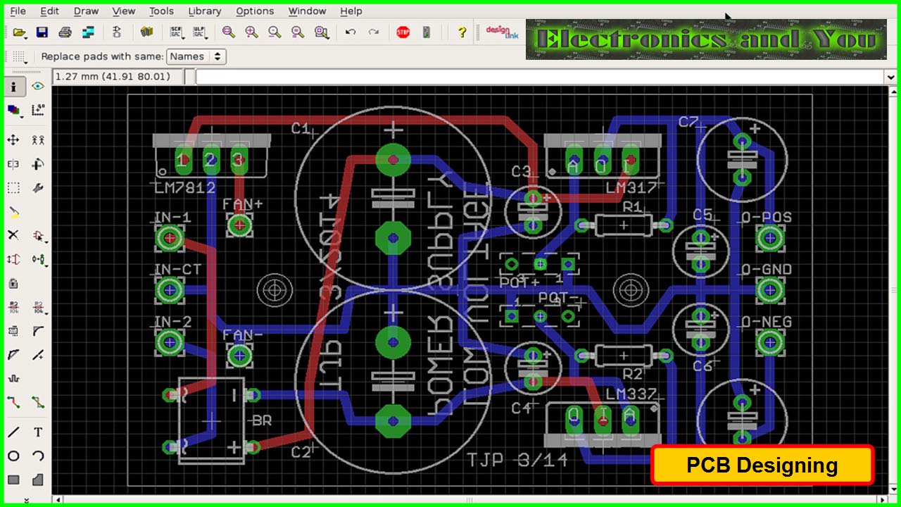
In our example we will use the led flasher circuit and design its pcb.
Pcb design process steps pdf.
Step by step pcb designing tutorial.
The pcb layout and design has a major impact on the way in which a circuit work and therefore if the printed circuit board is designed in an effective way then the circuit will perform more reliably and within its specification.
Can continue the process still using tina 7 design suite and later versions since pcb design is now an integral part of the program.
Let s learn how to design a pcb by working through a few examples.
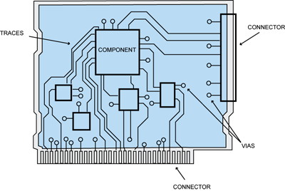
Cad flow for pcb design.
What is a multilayer pcb.
Different pcb design software possibly calls for different gerber file generation steps they all encode comprehensive vital information including copper tracking layers drill drawing apertures component notations and other options.
How to design a pcb step by step pictorial views with example pcb of led flasher circuit what is pcb printed circuit board.
Follow my tradition schematic capture place components route traces gen gerbers fab.
Knowing how to design a printed circuit board pcb is a key element of any electronic circuit design process.
2 1 generating a schematic refer to the eagle manual available at www cadsoft de for specific instructions on.
P cad pcb user s guide i table of contents chapter 1 introduction to p cad pcb p cad pcb features 1.
The steps will be described in the following section.
Circuitry with pre defined electrical function.
The pcb design process a summary of a lot of information place components route traces fab.
Has a variety of chemicals in the store for pcb fabrication process.
Pcb manufacture and design always start with a plan.
Iteration eagle pcb www cadsoft de generate gerbers schematic capture.
Has facility for producing deionized water which is used in plating purpose.
The beginning step of any pcb manufacture is of course the design.
A platform for components.
All aspects of the pcb design undergo checks at this point.
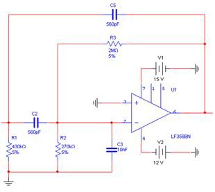
The circuit should be fully designed with all the parts sourced before proceeding to the pcb design.
The first item needed when building any electronic product but often ordered last.
Introduction to multilayer pcb s the green thing with holes in it.
Iit kanpur pcb design guide sheet page 16 of 26 the pcb lab.
The designer lays out a blueprint for the pcb that fulfills all the requirements as outlined.